
Semiconductor manufacturing is becoming increasingly complex as miniaturization advances, new materials, and assembly and packaging technologies are introduced.
Improving semiconductor manufacturing

through dynamic force, pressure and acceleration measurement
What challenges does semiconductor manufacturing face?
Miniaturization increases sensitivity
Smaller geometries increase susceptibility to mechanical stress and micro-vibrations that remain invisible to standard inspection tools.
3D packaging adds complexity
Advanced packaging and die stacking introduce multi-axis mechanical loads that static sensors cannot characterize.
Stress events are millisecond-scale
Yield-critical mechanical events occur within milliseconds, which is far below the capture rate of conventional inspection.
End-of-line inspection detects too late
Optical and electrical inspection often finds defects after value has already been added - scrap is unavoidable.
How measurement solutions from Kistler solve challenges in semiconductor manufacturing
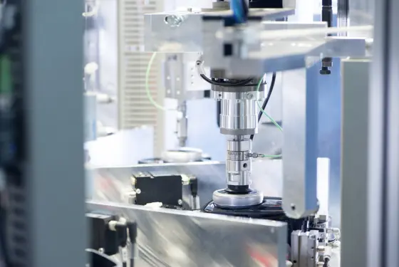
Dynamic force, pressure, and acceleration measurements are critical, as many yield‑relevant mechanical stress events occur within milliseconds and cannot be detected by static or end‑of‑line inspection methods. Piezoelectric measurement technology ensures high-resolution monitoring and control of the forces applied during semiconductor manufacturing processes - no matter how small.
By making physical dynamics visible in real time, Kistler enables semiconductor manufacturers to:
Higher yield, lower scrap
Inline process deviations are caught before they propagate - protecting product quality at every step.
Closed-loop downforce control
Real-time force feedback enables active process correction at microsecond resolution for tighter tolerances.
Faster tool qualification
Full process transparency compresses ramp time for new tools, nodes, and advanced packaging processes.
Micro-vibration detection
High-frequency accelerometers capture machine-induced vibrations that degrade bond strength and lithography.
Full product traceability
Every process event is time stamped and linked to individual units for complete lot traceability and audit readiness.
Stable long-term operation
Piezoelectric technology maintains calibration stability across thermal cycling, vacuum, and cleanroom environments.

New white paper: enhancing process control in semiconductor manufacturing
Download the white paper to discover how piezoelectric force monitoring improves process stability, yield, and quality.
Selected use cases for yield and quality optimization in semiconductor manufacturing
Learn how Kistler supports semiconductor manufacturers in overcoming today’s production challenges.
Kistler supports the complete semiconductor manufacturing chain
From wafer fabrication through final test, Kistler provides a measurement chain for every critical stage.
Featured products

Handheld charge amplifier and transmitter monitor
Data recording, insulation testing and quality assurance – the easy way
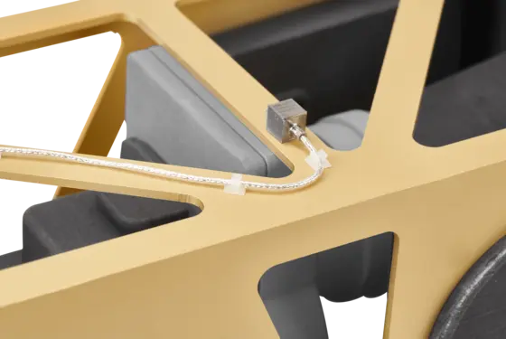
KiVibe Miniature triaxial IEPE accelerometer
The perfect fit for vibration measurements on lightweight structures and in tight spaces
Need a consultation?
Our experts are just a click away.
![[object Object]](https://kistler.cdn.celum.cloud/SAPCommerce_Document_Preview/961-140e.webp "Optimized semiconductor production")
![[object Object]](https://kistler.cdn.celum.cloud/SAPCommerce_Document_Preview/961-500e.webp "Using piezoelectric sensors to measure dynamic force in semiconductor applications")