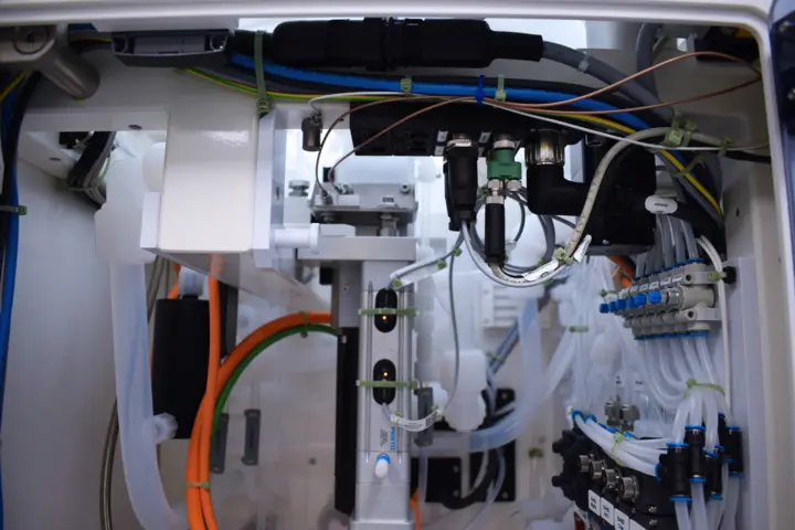
Complex inner workings: AP&S wafer cleaning and surface processing systems include large numbers of components that present a challenge for predictive maintenance.
tepcon's software experts have launched a partnership with the new Kistler Digital Solutions Lab. The goal: to integrate predictive maintenance capability into the wet process systems developed by AP&S, tepcon's sister company. This development project in the semiconductor production sector takes machine learning as the basis for creating intelligence with predictive ability, independently of the individual plant.
The semiconductor sector is one of the most complex of all industries: circuits and microstructures such as MEMS are becoming more compact and more powerful, while production technology is also evolving at a relentless pace. Nowadays, 400 to 1,000 individual steps are needed to manufacture just one single chip – resulting in complex value chains that span the globe and are difficult to understand and manage.
One of the pieces in this intricate jigsaw puzzle is AP&S, a company based at Donaueschingen in the extreme south-west of Germany. They specialize in manufacturing wet process systems that are used for cleaning and surface processing (etching, stripping and plating) of wafers and substrates.160 employees across the globe develop and manufacture equipment here in two segments: Single Wafer Processing and Batch Processing. The AP&S portfolio also includes services such as system repairs and complete overhauls.


![An artificial intelligence emerges [object Object]](https://kistler.cdn.celum.cloud/SAPCommerce_Document_Preview/961-398e.webp)